Designing with Precision: Integrating 25v 1000uf SMD 4 x 5.4mm Electrolytic Capacitor KiCad for Compact PCB Layouts
In the evolving world of electronics design, every millimeter of space on a printed circuit board (PCB) counts. As devices continue to shrink and performance expectations rise, engineers and designers must carefully select components that not only meet electrical requirements but also fit seamlessly into a compact form factor. One such essential component in power management and filtering applications is the 25v 1000uf smd 4 x 5.4mm electrolytic capacitor kicad. When integrating this specific capacitor into a design using KiCad, a popular open-source PCB design tool, precision and planning are crucial to ensure a functional and manufacturable layout.
This article provides a comprehensive guide to incorporating this small yet powerful component into compact PCB layouts, focusing on footprint creation, electrical performance, and layout optimization in KiCad.
Understanding the 25v 1000uF SMD 4 x 5.4mm Electrolytic Capacitor
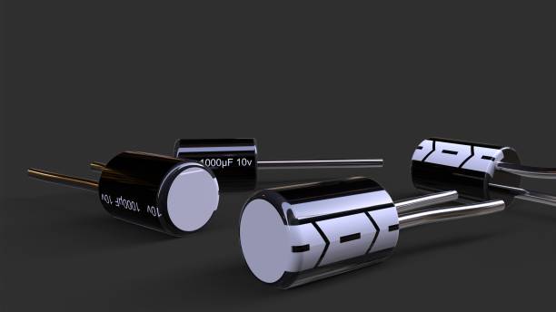
The 25v 1000uF SMD electrolytic capacitor is a surface-mount device designed to provide high capacitance in a compact footprint. Measuring 4mm in diameter and 5.4mm in height, this capacitor is commonly used in applications requiring energy storage, voltage smoothing, and power decoupling, especially in densely populated PCBs like portable electronics, embedded systems, and miniaturized power supplies.
Key Features:
- Rated Voltage: 25V
- Capacitance: 1000µF
- Mounting Type: SMD (Surface Mount Device)
- Dimensions: 4mm (Diameter) × 5.4mm (Height)
- Polarity: Polarized (Requires proper orientation)
Despite its small size, this capacitor is capable of handling moderate current ripple and storing significant energy, making it ideal for switching regulators, audio circuits, and microcontroller power rails.
Step-by-Step Guide: Using the Capacitor in KiCad
1. Footprint Creation and Symbol Selection
KiCad’s default libraries may not contain an exact footprint for a 25v 1000uF SMD 4 x 5.4mm electrolytic capacitor, so you may need to create a custom footprint.
Creating a Custom Footprint:
- Open KiCad’s Footprint Editor.
- Set the pad layout according to manufacturer specs: generally two rectangular pads, spaced appropriately to accommodate the 4mm diameter.
- Add silkscreen outlines and a polarity marker. Polarity is crucial in electrolytic capacitors.
- Ensure the pad dimensions provide sufficient solder area and comply with IPC-7351 standards for solder joint reliability.
- Save the footprint under a recognizable name like Cap_Elec_4x5.4_SMD.
For the schematic symbol, you can use a generic electrolytic capacitor symbol and link it to your custom footprint.
2. Electrical Considerations
Before placing the capacitor in your schematic:
- Verify that 25V is above your circuit’s maximum voltage.
- Ensure the 1000µF value is suitable for your application—whether for bulk decoupling or noise suppression.
- Evaluate equivalent series resistance (ESR), as it affects ripple performance and power dissipation.
In power supply applications, lower ESR values typically provide better filtering.
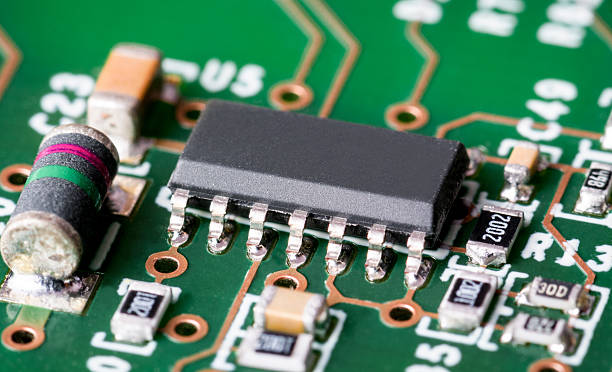
Layout Strategies for Compact Designs
Once the component is included in your schematic and netlist, it’s time to lay it out in KiCad’s PCB editor. Compact designs require careful planning to avoid signal integrity issues and component interference.
1. Optimal Placement
- Near Power Rails: Place the capacitor as close as possible to the power input or IC supply pins to minimize parasitic inductance.
- Polarity Alignment: Observe the positive and negative pad orientations. Reversed installation can lead to capacitor damage or explosion.
- Thermal Relief: For high-current applications, connect the capacitor’s pads to wider copper pours for improved thermal and current handling.
2. Via and Trace Design
- Use thick traces (≥0.5mm) or copper pours to connect to the capacitor, especially in power filtering circuits.
- If routing to multiple layers, use via stitching to minimize ground bounce and ensure low impedance.
3. Clearance and Isolation
- Maintain adequate spacing from high-speed signal lines to reduce EMI coupling.
- Keep high-current return paths as short and direct as possible, ideally under the capacitor’s placement.
Simulation and Verification
KiCad integrates with tools like ngspice for basic circuit simulations. While simulating electrolytic capacitors can be challenging due to limited real-world ESR and leakage current data, you can still model basic filtering behavior:
plaintext
CopyEdit
.model ECap C C1 N001 N002 1000u R1 N002 0 0.1 ; ESR ~ 0.1 ohms
Simulations help validate the capacitor’s role in decoupling noise and handling transient load steps.
Thermal and Mechanical Considerations
Electrolytic capacitors are sensitive to temperature. In compact PCBs:
- Avoid placing the capacitor near heat sources like MOSFETs or voltage regulators.
- Maintain proper ventilation or use thermal vias to help dissipate heat.
- Ensure the capacitor is not subjected to mechanical stress during reflow soldering. Use courtyard lines to define safe assembly areas in the footprint.
Bill of Materials (BOM) Management and Fabrication Tips
When preparing for manufacturing:
- Double-check that the part number (e.g., from Panasonic, Nichicon, or Rubycon) matches the physical footprint.
- In your BOM, include full part specs, tolerance, ESR, and packaging type (e.g., tape & reel).
- Use KiCad’s BOM plugins or custom scripts to output clean, supplier-ready spreadsheets.
Before finalizing your design, use KiCad’s 3D viewer to visually inspect capacitor placement and height clearance. This is particularly useful in enclosures with vertical space constraints.
Final Checklist for Integrating 25v 1000uf smd 4 x 5.4mm electrolytic capacitor kicad:
- Schematic symbol linked to a custom footprint
- Correct polarity marking and orientation
- Adequate pad size and spacing
- Suitable ESR and voltage ratings
- Thermally optimized copper pours or wide traces
- BOM includes accurate part numbers
- Simulated or validated for decoupling performance
- 3D footprint confirms enclosure fit
Conclusion
Designing with Precision: Integrating 25v 1000uf SMD 4 x 5.4mm Electrolytic Capacitor KiCad for Compact PCB Layouts is not just about component selection—it’s about thoughtful engineering. With the right practices in place, KiCad becomes a powerful ally in crafting efficient, space-saving, and reliable circuits. This specific capacitor, despite its compact size, can significantly enhance the stability and performance of your electronic design when properly integrated.
Whether you’re building a low-noise amplifier, a compact power supply, or a miniature IoT device, mastering the integration of such capacitors in KiCad will refine your ability to deliver robust and manufacturable PCBs.


Post Comment