Top Mistakes to Avoid When Placing 20V 1000uF SMD 4 x 5.4mm Electrolytic Capacitor KiCad PCB Layouts
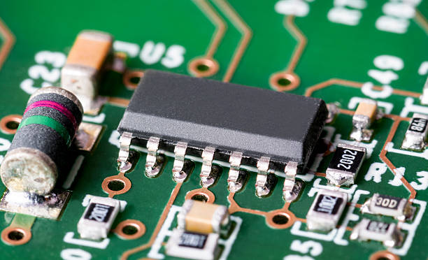
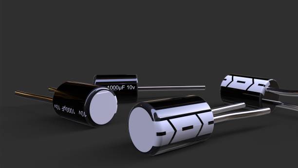
When working on compact and efficient PCB designs, electrolytic capacitors play a critical role in ensuring signal integrity and power stability. One common component used in power filtering and decoupling is the 20v 1000uf smd 4 x 5.4mm electrolytic capacitor kicad. While it’s a compact capacitor ideal for tight spaces, placing it incorrectly in your KiCad PCB layout can cause significant performance issues—or even render your board inoperable.
In this guide, we’ll focus on the top mistakes to avoid when placing 20v 1000uf smd 4 x 5.4mm electrolytic capacitor in KiCad PCB layouts, and how to mitigate these errors through smart design practices. Whether you’re a beginner or an experienced PCB designer, these insights will help improve the reliability and manufacturability of your projects.
1. Incorrect Footprint Selection in KiCad
One of the most fundamental mistakes is choosing the wrong footprint for your 20V 1000uF SMD capacitor. While the physical size is specified as 4 x 5.4mm, selecting a generic or mismatched footprint may lead to soldering issues or clearance problems.
Avoid this by:
- Matching the footprint exactly with the manufacturer’s datasheet.
- Verifying pad size, pitch, and thermal pad requirements in the Footprint Editor.
- Using a 3D model to visually inspect how it will look on the PCB.
Even a millimeter difference can cause placement issues, especially when working with pick-and-place machines in manufacturing.
2. Neglecting Polarity Markings
SMD electrolytic capacitors are polarized components. Unlike ceramic capacitors, they must be placed with the correct orientation; otherwise, they can explode or fail silently.
Common polarity errors include:
- Incorrect schematic symbol setup.
- Flipping the component during layout without updating the net assignments.
- Misinterpreting the marking on the PCB or footprint.
Fix this by:
- Always double-checking the anode (positive) and cathode (negative) pads.
- Ensuring the silkscreen clearly marks the cathode side.
- Reviewing the KiCad 3D model to verify orientation.
3. Placing the Capacitor Too Far from the Power Source
The 20V 1000uF SMD capacitor is often used for power decoupling or smoothing. However, if it’s physically placed too far from the IC or power regulator it supports, it loses much of its effectiveness due to trace inductance and resistance.
To avoid this:
- Place the capacitor as close as possible to the power pin or regulator output.
- Use short and wide traces to minimize impedance.
- In high-current designs, consider using polygon pours or planes to connect the capacitor.
4. Poor Thermal Relief or Via Placement
High-capacitance SMD components can generate or absorb significant heat, especially in power circuits. Designers often forget to provide adequate thermal relief, which can lead to overheating or inefficient soldering.
Common errors include:
- Connecting the pads directly to large copper pours without thermal spokes.
- Skipping thermal vias on multilayer PCBs.
Prevention tips:
- Enable thermal relief in zone settings in KiCad.
- Use multiple vias to ground or power planes for better current flow and heat dissipation.
- Simulate thermal performance using tools like KiCad’s external integrations.
5. Ignoring the Height Profile in Dense Layouts
The 5.4mm height of the capacitor may not seem like much, but in tight enclosures or multi-board assemblies, it can interfere with casing or connectors.
Designers often fail to:
- Include 3D enclosure models during layout.
- Check height restrictions from adjacent modules.
To fix:
- Use KiCad’s 3D Viewer to examine spatial fit.
- Set height limits using the mechanical layer or a constraint layer.
- Clearly document part height in design notes for production teams.
6. Improper Grounding or Floating Capacitor Pads
A capacitor that isn’t correctly tied to ground or power nets becomes useless—or worse, causes floating nodes that destabilize your circuit.
Frequent causes:
- Assigning the wrong net label in the schematic.
- Forgetting to connect a pad during routing.
Avoid this by:
- Running DRC (Design Rule Checks) in KiCad before finalizing the design.
- Using highlight net features to visually confirm connections.
- Never leaving a capacitor pad unconnected unless explicitly intentional (e.g., for testing).
7. Overcrowding and Violation of Clearance Rules
Trying to cram a large 1000uF capacitor in a small space without proper clearance can result in solder bridging, shorts, or manufacturing issues.
Common clearance issues:
- Pad-to-pad or pad-to-trace spacing violations.
- Capacitor interfering with nearby components during reflow.
Solutions include:
- Respecting manufacturer-specified minimum clearance distances.
- Using KiCad’s clearance rules and zone settings effectively.
- Running design rule checks (DRC) with realistic spacing constraints.
8. Using Auto-Router for Sensitive Power Paths
While KiCad has routing aids and external autorouter support, relying solely on auto-routing for power components like electrolytic capacitors can lead to non-optimal paths with excessive inductance or EMI issues.
Instead:
- Manually route critical power and ground traces.
- Use polygon fills for return paths.
- Prioritize symmetrical and direct connections over automatic meandering paths.
9. Failing to Plan for Rework or Replacement
Electrolytic capacitors, especially in consumer products, may eventually degrade or fail. If your design doesn’t consider accessibility for replacement, you’re asking for long-term issues.
Oversights include:
- Placing the capacitor under heatsinks or large connectors.
- Not leaving enough solder mask clearance around pads for rework tools.
Better design practice:
- Leave at least 1-2mm clearance around the component for soldering iron access.
- Add test points or vias nearby for voltage testing and diagnostics.
10. Skipping Library Version Control and Documentation
Last but not least, failing to document which capacitor variant was used (especially if you create a custom KiCad footprint or symbol) can cause bill-of-material errors or delays in production.
Fix this by:
- Maintaining a well-documented library with proper version control (e.g., using Git).
- Linking the KiCad component to a specific manufacturer part number (MPN).
- Including capacitor specs like ESR, ripple current, and tolerance in your BOM.
Conclusion
Avoiding these common mistakes when placing a 20v 1000uf smd 4 x 5.4mm electrolytic capacitor kicad in your KiCad PCB layout can greatly enhance the performance, reliability, and manufacturability of your design. By paying attention to footprint accuracy, placement proximity, polarity, thermal management, and layout spacing, you’ll not only prevent costly reworks but also create a more robust and production-ready circuit.
Always treat large capacitors as critical components—not just in electrical terms but also in layout planning. With a smart approach and attention to detail, your KiCad PCB layout will be as precise as it is functional.


Post Comment